These are notes and schematics to help you understand how the TE-WB Version 2A0 works. Please note that all images and text are Copyright 2003..7 © Tech Edge Pty. Ltd.
|
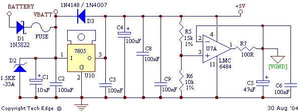
Reverse polarity protection to the unit is provided by Schottky diode D1, while fast Zener D2 (Tranzorb) provides transient suppression. The PCB mounted 3 Amp fuse provides protection against internally generated fault conditions. C1 through C4 filter and suppress vehicle electrical noise around the 5 volt 7805 (U10 TO220) regulator. Diode D3 protects the regulator from shorts across the battery input. Op-Amp U7A (LMC6484) generates a 2.0 V Virtual Ground (VGND) which is used as the reference point for the analogue interface to the sensor. C5 and C6 provide filtering and noise suppression while R7 provides short circuit protection in the event of a fault. |
|
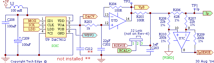
The sensor is an analogue device but it is controlled by digital signals. The 12 bit dual DAC (Digital to Analog Convertor, DAC7612) produces a voltage in the range of 0 to 4.096 volts (in steps of 1 mVolt). The DAC's A section output is buffered by unity gain op-amp U7D and then applied to the sensor's Ip drive to produce a pump current which flows though resistors R205 and R206. This arrangement gives an Ip Voltage of +/- 2.0 Volts (relative to VGND) and this provides the positive or negative pump current to control the sensor's pump cell in the rich and lean regions. The B section of the DAC drives the linear wideband output WBLin (see section output below). The DAC's power supply is decoupled from the other digital circuitry via Inductor (L2) and capacitors C208 & C209. The DAC is an SPI device (see microcontroller section below). The pump cell is a current operated device and the Ip generated by the DAC's output voltage is calculated by measuring the voltage developed across 62 ohm sense resistor R206. For the LSU sensor, its calibration resistor acts in parallel with R206 (shunt J2 must be in the 2-3 position). Differential amplifier U7 senses the pump current and produces a voltage IpSense. Note that on the Rev-4 PCB the J2 link has been removed, and on the Rev-2/3 PCBs the link should always be in the 2-3 position. |
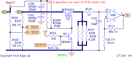
R101 to R104 constitute two voltage dividers to sense the H+ & H- heater voltage. These voltages are fed to the muxes (see 74HC4052 mux sections below).
Heater current is sensed by measuring the voltage developed across resistors R107 to R109. U6B amplifies and filters this voltage to produce signal Ih.
FET Q3 switches on and off (ie. PWM control) to control the average current to the heater. The gate drive transistor Q4 is controlled by the microcontroller and ensures the FET switches quickly and cleanly. C104 (SNUB1) and C105 (SNUB2) provide a path for switching transient currents and work to reduce the effect of the large heater switching currents and induced voltages on other sensitive parts of the circuit.
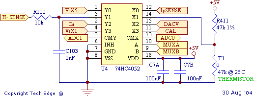
The dual 4 to 1 line mux U4 (74HC4052) allows two groups of four signals to be sensed by the microcontroller's two ADC input lines ADC0 and ADC1.
Vsx5, Ih, Vsx1, IpSense , DACV & Cal (VGND) voltages are sensed as well as H- via filtering provided by R112 and C103.
The thermistor T1 with nominal resistance of 47k at 25°C provides the ability to measure the onboard temperature of the WBo2 unit and thus provide cold junction compensation for the thermocouple readings.
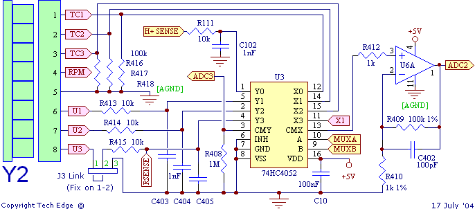
Another mux, U3 is used for logging externally sensed data which include three K-type thermocouple channels (TC1 to TC3) and three 0 to 5 Volt analogue inputs U1 to U3.
A single op-amp U6A with a gain of 101 amplifies the signal from all the thermocouples. This amplifier is single ended and is thus a compromise as better performance results from a differential input amplifier (but there is a lack of space on the Y2 connector for more input pins). C402 provides some measure of thermocouple filtering. Note that software processing and filtering of these signals, and the thermistor signal, is required to produce a measure of the temperature sensed by the thermocouple(s).
Analogue user inputs U1 to U3 have a very simple filter, as does the H+ Sense input. The Rsense input was originally intended for L1H1 calibration resistor sensing but this has been dropped and the J3 link should be fixed in the 1-2 position so that user input U3 can be correctly sensed.
Sense Cell Voltage Amplifier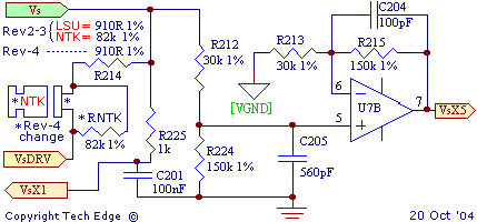
The Vs Drive (VsDRV) signal is used to sense the impedance (know as Ri) of the Vs Sense cell. As the LSU (Bosch) and the L1H1 (NTK) Vs cells have very different characteristics, a different mechanism is employed for the NTK cell. For the NTK sensor, the LSU's 910 ohm resistor change to around 82 k. On the Rev-2/3 PCB the resistor R214 must be physically swapped when changing between NTK and Bosch sensors. On the Rev-4 PCB there is a link (labelled NTK) that should be removed for the NTK, and added for the LSU (yeah, it should be called the LSU link!). Rev-4 also adds the 82k resistor RNTK and removes the requirement that R214 be changed (R214 is fixed at 910R on the Rev-4 PCB). Note that the LSU/NTK PCB jumpers (these are the links J2 in the "DAC, Ip Buffer & Current Sense" secion above, and J3 in the previous section) do not function as was originally envisaged and should be fixed in the LSU position according to the silkscreen information under the fuse. |
* 470nF Capacitor for Low Pass RC filter.
* Schmitt Trigger
* Inverting Monostable with 1mS pulse
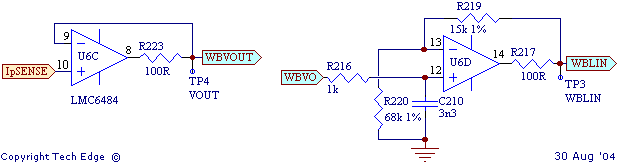
U6C buffers the signal from the differential IpSense amplifier to produce the raw WBVout. This signal is used for testing as it is not calibrated.
The CPU processes the IpSense signal in software to produce WBlin. The 12 bit DAC (see above) generates up to 4.096 Volts. U7B has a gain of (68+15)/68 and gives WBlin a maximum value of 5.000 Volts in steps of 1.2 mVolts. Note the 100 ohm resistor R217 is used to limit short circuit output current and is wired in the feedback loop to avoid changes in the output voltage when low impedance loads are used.
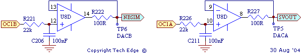
The CPU's 10 PWM generator is used to produce the SVout and NBsim signals using op-amps section U8C & U8D. A simple single pole filter adds some smoothing and filtering to each output.
|
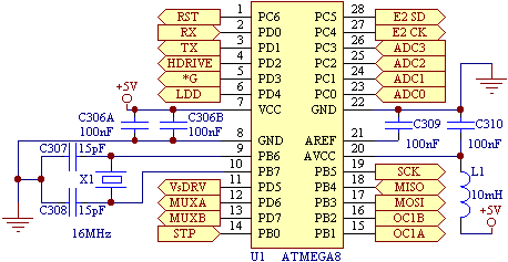
An Atmel Mega-8 (16 Mhz) RISC CPU provides the unit's intelligence. The schematic shows the crystal, decoupling capacitors, and the inductor for filtering the CPU's analogue ADC reference. |
|
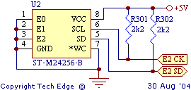
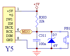
The Mega-8's I2C (two wire) bus interfaces to an ST-M24256-B 8 pin 256 k bit (32 k byte) EEPROM. It is used to store data when on-board logging is active. The two 2.2 k resistor are the required pullup for the open-drain SCL and SDA lines. A 100,000 programing cycle & 40 year data retention is claimed for the device. Note: Rev-3 of the PCB fixes a previous error where E2-CK and E2-SD lines from the processor were swapped. The Rev-2 PCB can be easily updated by cutting two traces and adding two wire links. On-board logging is controlled by press button switch PB1 (refer to logger details here). Components R303 and C311 interface the switch to the processor and optional zener (not supplied in kits, and solders to the bottom of the PCB) is for situations where a remote logging switch is used. From Rev-3 there is a position on the PCB for PB1. |
|
LEDs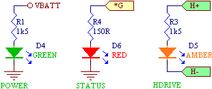
|
|
RPM Input & Jumpers J1 & J4Note that the Rev-2 and Rev-3 PCBs have slight differences. Rev-4 PCB removes jumper J2, and we suggest you use a wire link for J3 (in the 1-2 position) 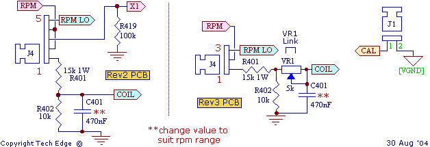
note : it's very important to have the J4 jumper in the right position if you are measuring RPM! |
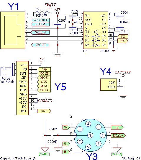
The serial driver (ST202) includes a charge pump device to produce a true (-)ve RS232 rail. Y1 is an RJ45 connector and requires an adapter cable for connection to a PC or Palm (see RS232 Data Cable below). Y1 also brings out the narrowband, wideband and SVout (for the display) analogue signals. An external splitter board is available that splits the single RJ45 into two (one for the display and another for a serial connector) as well as providing a connection to the WBlin and NBsim signals. Y5 is a general purpose connector that was intended for a possible future integrated display. Y5 contains the AVR's ISP signals. Pins 2 and 3, under firmware control, provide the possibility of a forced re-flash should the CPU's program memory become corrupt. Y3 is the 8 pin sensor connector. See below for how the sensor is connected to Y3. Y4 is the battery power connector (Molex Mini-Fit). |
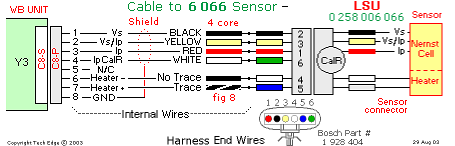
This is the cable from the circular 8 pin connector (female end of Y3) to the LSU sensor connector. The connector shown is for the 0 258 006 066 sensor. See also the LSU information page with pinouts for other LSU sensors and the NTK (L1H1) sensor cable pages.
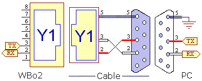
This is the serial data cable from the RJ45 connector (female end of Y1) to the RS232 DB9 connector. The red wire carries commands from the external device (PC, etc) and the white wire carries logging data and responses from the WB unit itself.
For PDA use (ie. Palm, etc.) a different cable connection is required. Refer to the Palm Logging page for more information.
We appreciate your feedback on the content and any corrections necessary to this article.