Previous | WBo2 | LD01 Info | LD01 Kit | TE-5301 | Older 5300 | Original FMD
|
|
|
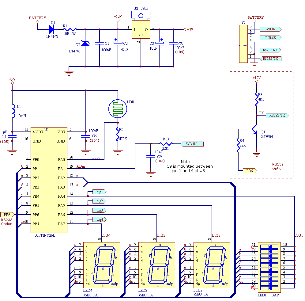
The LD01 may be used in a number of simple display applications. Normally the display will be built with a subset of all possible parts installed. In particular, for the LD01 wideband display, just the parts shown in the parts list below are installed. The full LD01 schematic can be accessed from the image/link at left. All components that can be installed are shown in this schematic. |
LD01 WB schematic
|
|
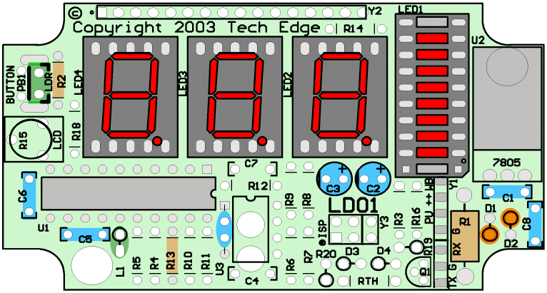
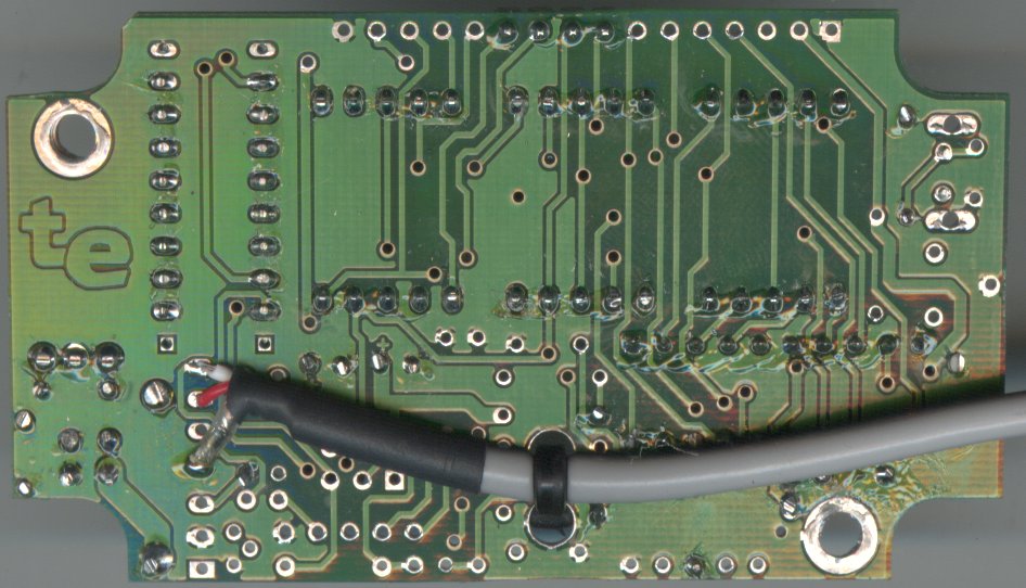
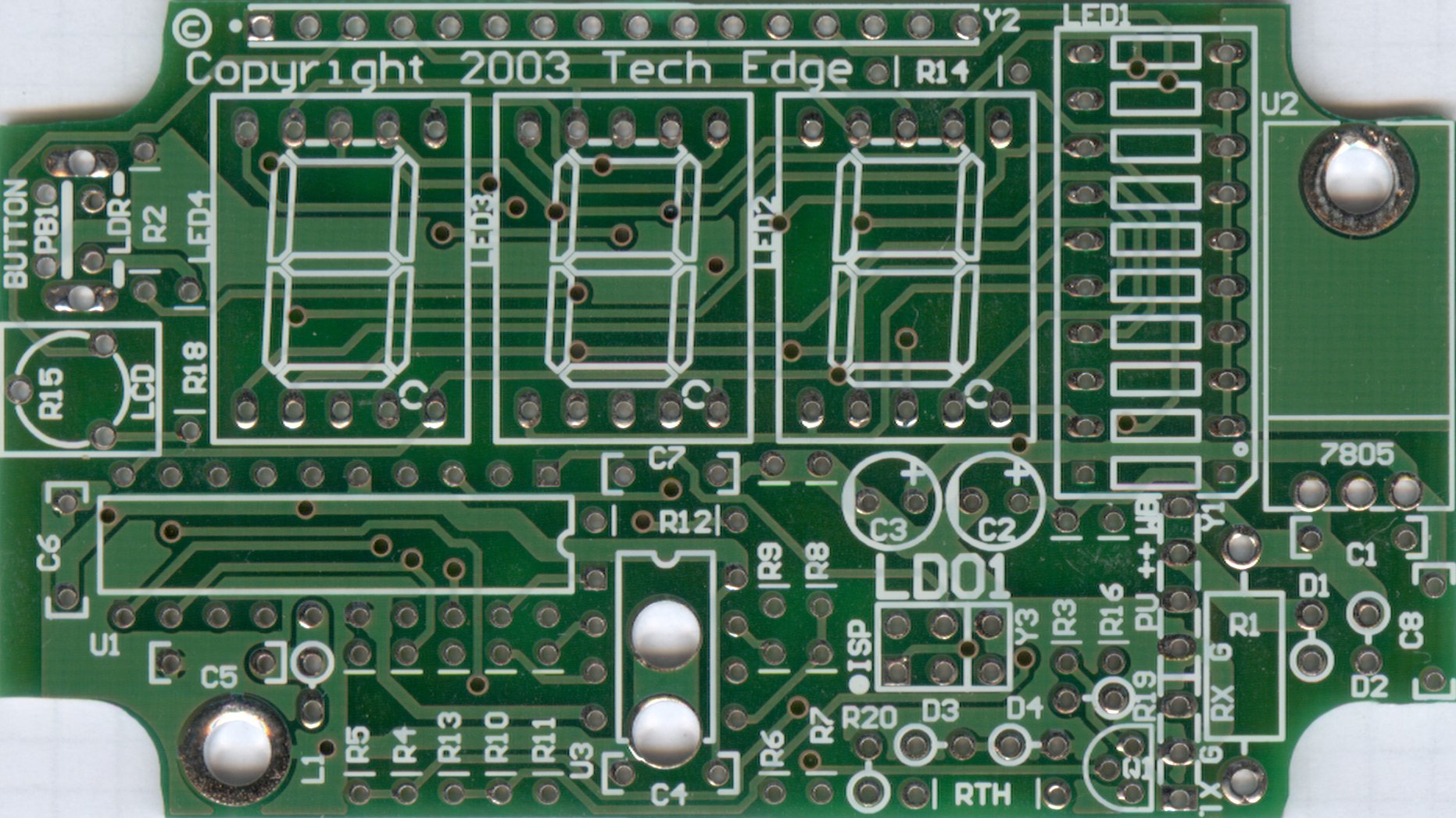
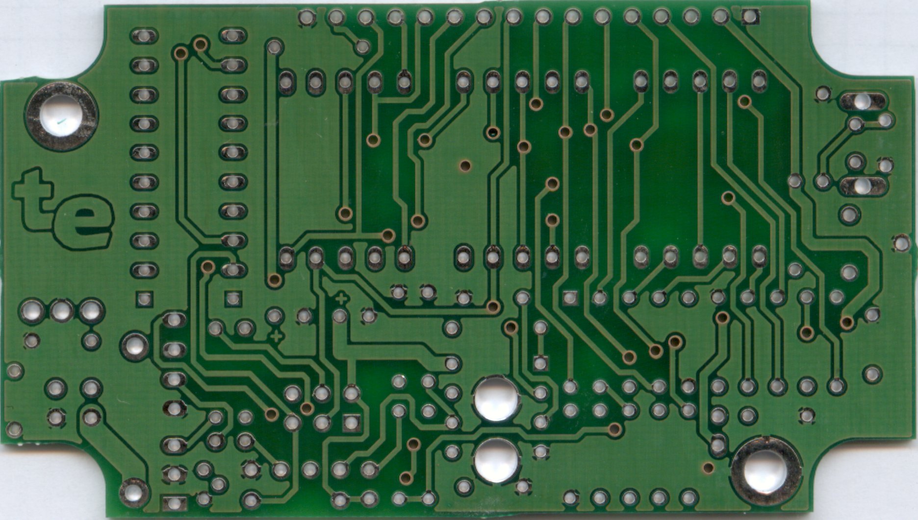
At right is the component overlay for the wideband version of LD01. Note that C9 is inserted between pins 1 and 4 of U3 (U3 is not installed). Note also the two holes under U4 for using a cable tie to anchor the power/signal cable on the other side of the board. The optional RS232 components are not shown in this image although these parts are included in kits. See below for more RS232 information. For reference we have an image of the front of LD01 PCB [393 k byte], and the back of LD01 PCB [316 k byte]. |
|
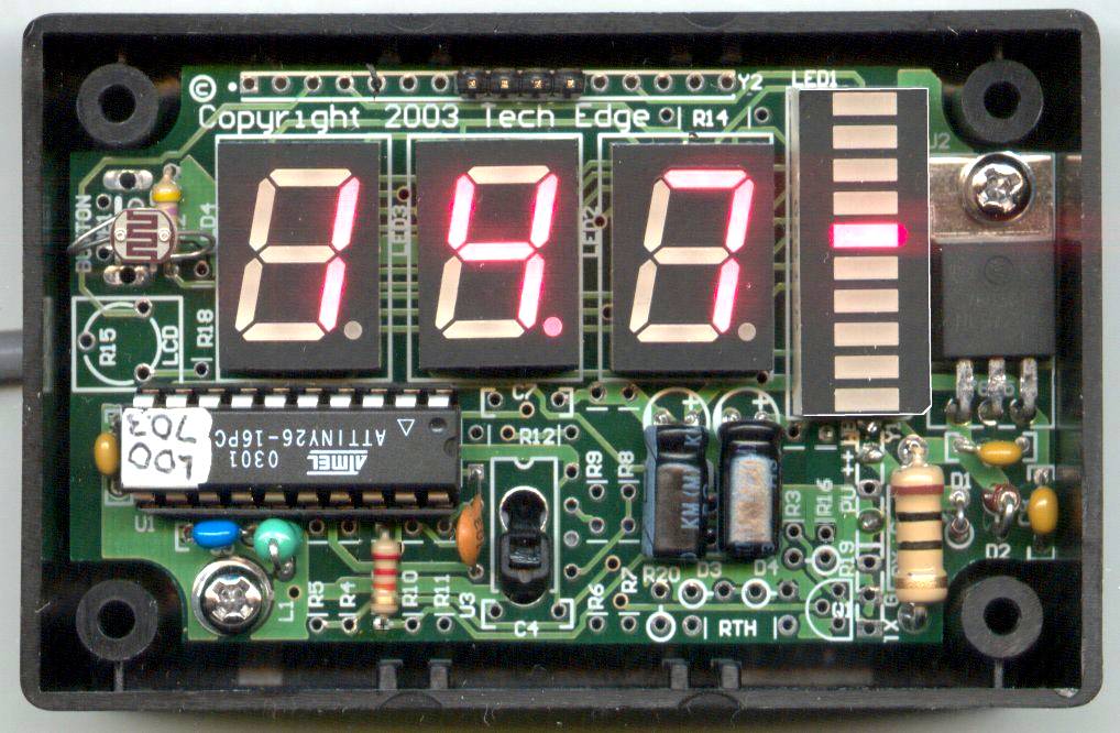
The single PCB used in the kit is shown in this image with just the parts required for the standard LD01 installed (the LEDs are showing 14.7). The optional RS232 components are not shown. Take special note of the LED orientation. The dots (decimal points) for the 7 segment displays must be at the bottom as shown. The bevel on one edge of the 10 segment LED bar must be closest to the 10 Ohm resistor. Note also the ATTiny26's orientation - it is "upside down" with pin 1 at the top right of the socket. |
|
This shows one way to connect the cable to the PCB (prebuilt units are supplied this way). The other way involves using the header pins (x4), socket and terminals that are supplied with the kit. If you use the header then note that it mounts on the soldered side and should be soldered after other components have been installed. |
|
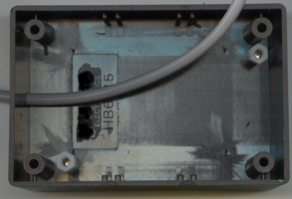
This image shows the two 15 mm nylon spacers installed in the case using two countersunk bolts. Remember to insert the cable (with pre-attached RJ45) through the side of the case before soldering to either the terminals (for pin and socket connection), or direct to the PCB. If you have a 5301 style LD01 kit then you will also have a DB9 and backshell that you will have to attach to the cable. (in this case also refer to the TE-5301 kit) |
|
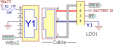
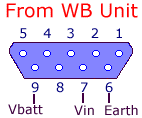
This schematic shows the cable from WBo2 to LD01. Kits are supplied with the shielded 2 core cable pre-crimped to the modular 8 pin RJ45 plug. You should check that the cable has been crimped properly. The cable's shield (copper braid = RJ45-p5) is the GND, red is battery power in (VBatt) and white is WBin (Svout). |
|
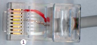
In this image of the above cable, note:
|
|
The LD01 (initial revision 0.0) has no calibration components, and no means of making any adjustments to span and offset (as did the 5301 display). In general the display should be accurately set to the correct AFR as the unit is inherently self calibrated. If you have a version 1.5 WB unit connected to the LD01 then you can change the 2.5SET control to get an accurate stoich AFR of 14.7 (do this according to the version 1.5's calibration procedure).
The following parts list is for the wideband version of the LD01 display. See below for special instructions if you want to build a 5301 display using the LD01.
CAPACITORS
10nF ceramic C9 (between pin 1 & 4 of U3) (marked as 103)
3 x 100nF monolithic C1, C6, C8 (marked as 104)
1uF monolithic C5 (marked as 105)
10uF (or 22 uF) electrolytic C3
47uF electrolytic C2
RESISTORS
10R 1W R1
470K R2
4.7K R3 (RS232 option)
2 x 22K R4, R13 (R4 = RS232 option)
INDUCTORS
10mH L1
SEMICONDUCTORS
AT-TINY26L U1
7805 (TO-220) U2
2N3904 Q1 (RS232 option)
1N4148 D1 reverse polarity protection.
1N4743 D2 12 Volt Zener.
10 LED BAR LED1
3 x 7SEG LED (C/A) LED2, LED3, LED4
MISC PARTS
Pre drilled black case with laser cut and silkscreened faceplate.
Red acrylic lens (optionally GREEN may be available)
LDR Light Dependent Resistor dimmer sensor
DIP20 SOCKET
2m 2 core shielded cable with RJ45 Jack (for WBo2 Rev 2.0 usage, cut off RJ45 for 5301 kit)
female DB9, DB9 backshell kit, cable tie (use for TE-WB rev 1.5 usage, or LD01 RS232 option)
4 Posn. 0.1" 90° HDR Y1 (optional use, see text)
4 Posn. 0.1" PLUG mates with Y1 (see above)
4 X TERMINALS mates with Y1 (see above)
2 x 15mm M3 nylon spacers (standoff for PCB from case)
2 x M3 6 mm round head bolts (bolts PCB to spacers)
2 x M3 star washers (under M3 bolts to PCB)
2 x M3 6 mm countersunk bolts (bolts spacers to case)
|
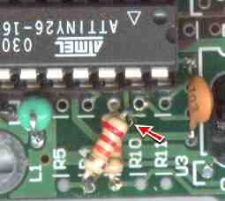
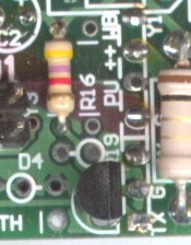
The LD01 kit is supplied with a transistor, two resistors, and a DB9 connector with backshell kit. This will allow you to add the optional RS232 output. We recommend you do not build the RS232 option - the native RS232 logging from the WBo2 is far superior to the very limited RS232 output from the LD01. We really designed this option so the LD01 was 100% functionally compatible with the existing 5301. The image at left shows the changes required to the PCB area close to the processor. Note that R4 (22 k) is soldered between one end of its original location and then to the PCB via (arrow points to this via) on the other side of the existing resistor (22 k R13). Make sure you don't solder to the nearby R10 pad. Important : the solder resist should be scraped from around the via hole before soldering. |
|
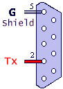
The image at right shows the additional 2N3904 transistor Q1 and resistor R3 (4.7 k) required. The point marked TX (closest to the edge of the PCB) is where the wire to the DB9 is taken from. The DB9 (female socket) is wired as shown at left. The copper shield wire of the cable is connected to the PCB beside the TX pin at the point with G label (for GROUND). Make sure you don't short TX to any other pins (we recommend you use heatshrink over it). Of course, you will have to drill a hole for the RS232 cable beside the existing cable from the WB unit. Make sure you drill the hole and thread the wire through before soldering both ends. |
|
Note: this document is added to and amended from time to time ....
 The LD01 display (
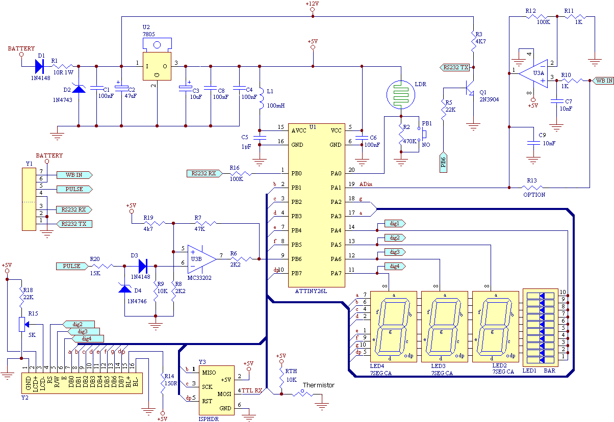