
The newer LD02B DIY kit is described here (introduced Dec. 2009)
- this document is for the original LD02 DIY kit.
|
|
|
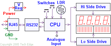
LD02 Design Overview
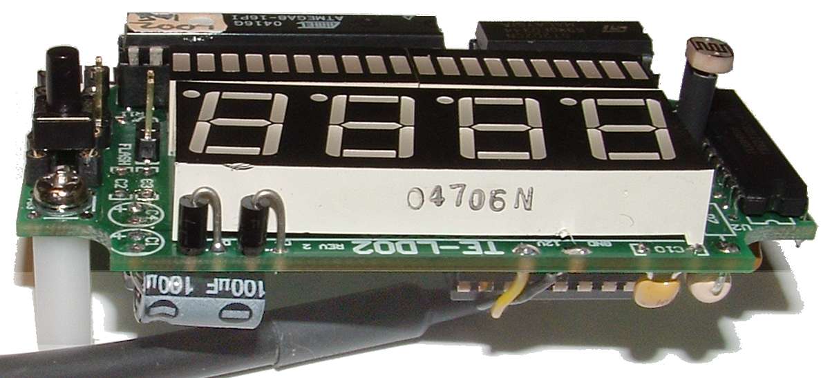
The image at left shows how the major components of the complete LD02 unit fit together.
Starting from the left is the RJ45 connector carrying power (& GND) to the unit as well as RS232.
The RS232 interface uses an ST ST202 (like the Maxim MAX232).
This is a bi-directional interface and the Tx line allow the unit to handshake with a PC for re-programming.
The Atmel Mega-8 CPU interprets the data frames from WBo2 and reads the
two |
|
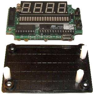
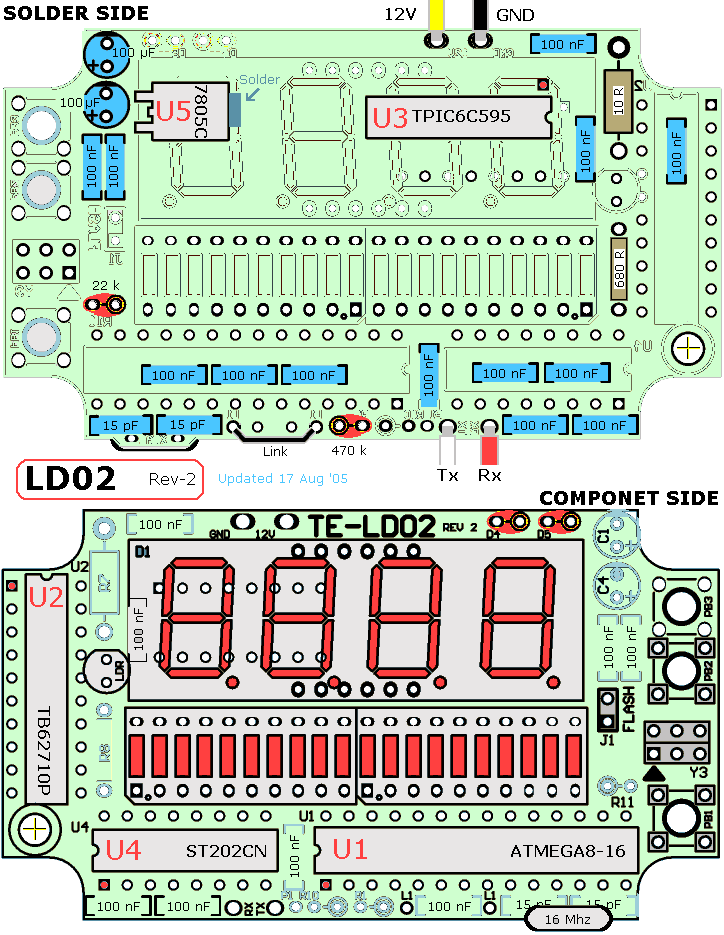
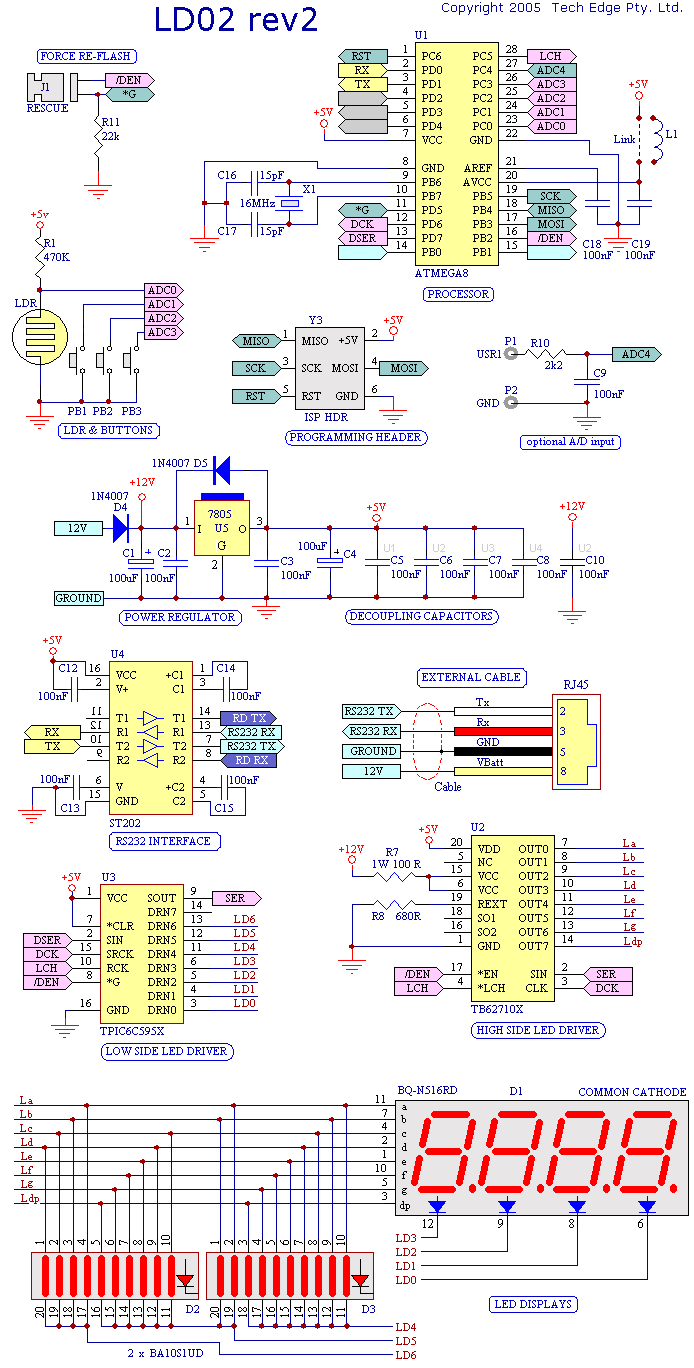
At left is the value and position (click on image at left, or here for pop-up) of all components installed on the PCB. We have also made available the PCB track layout as a PDF for fault finding should you get a board short. Because parts are on both side, the sequence that components are installed is important, so read the construction notes below too. The full LD02 schematic (click on image at right, or here for pop-up) is available for printing. We suggest you at least print the left (overlay) image, for use while assembling. |
The main PCB is shown in this image at right. The RS232/power cable is shown emerging from the underside (or solder side) of the PCB. Click to enlarge as a pop-up to enlarge it.
|
Unpack : First note that all the semiconductors are static sensitive. Do not take them out of their packaging until you are ready to install them later on. Now scroll down to the Parts List section at the bottom of this document. Check that you have all the parts there. If you also have a wideband or other kit, make sure you do not mix up any of the two kits as this will make your construction task so much harder. Note that here are two PCBs, the main one and the much smaller RS232 interface PCB. )
PCB Inspection : Inspect the main PCB for obvious faults or damage. Our boards are 100% tested for shorts and open traces but, although unlikely, PCB faults are still possible. Orientation(s) : Take special note of the LED orientation as attempting removal of a soldered LED module will destroy the PCB.
) Left, right, top, & bottom are correct when looking at the silkscreen side of the PCB with the "TE-LD02" label visible at the top.
Left, right, top, & bottom are correct when looking at the silkscreen side of the PCB with the "TE-LD02" label visible at the top.
The PCB's other side is called the solder side and shows the text © Copyright 2004. |
click for enlarged image |
Construction
click for enlarged image |
Solder side : Note that all the components on the solder side must be installed and soldered before the LED modules can be mounted. This is because the solder points are under the display modules. Begin by soldering components shown in the left image onto the PCB (click to enlarge as a pop-up. These include :
|
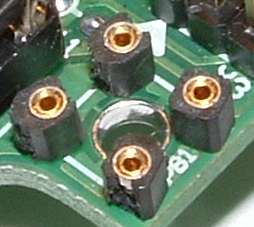
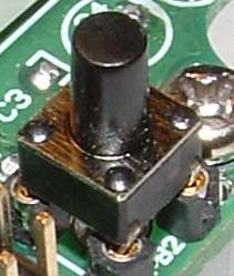
Firstly install the base for the switches. The switches (which were not available with longer shaft sizes) are not soldered directly to the PCB, but are pushed into machine socket pins that stand them off the PCB the correct distance. Begin by cutting the strip of 8 machined pins into individual pins. You will need sharp side cutters or even a Stanley knife (carefully, as the pins snap apart and fly around). Four pins are required for each button, and the left image shows these pins installed for the lower PB1 button. It's very important the pins are soldered flush with the PCB otherwise the press buttons may not install vertically. The image at right shows PB2 installed, but don't leave them in the sockets just yet. Next install J1 and Y3 - this pop-up image of the press buttons, showing the above two areas, may clarify what's involved. It shows that the strip of 8 header pins have been cut into 3 + 3 + 2 and installed to make up the Y3 and FLASH headers. |
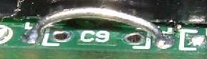
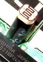
The 16 Mhz crystal is installed in the XTAL position - make sure you leave about 2 mm of lead between the PCB and the conductive base of the crystal's can (see image at right). The crystal should be just resting against the 28 pins socket so the loaded PCB just fits into its case. A link is installed between the two points L1 and L1, just in front of the U1 socket such that the link doesn't short out on the pins of C9. Note that C9 is not installed. |
It's time to solder in the single 4 digit module. Red is type BQ-N516RD, green is BQ-N512RD. Check these part numbers to ensure you have not been supplied the wrong parts. It is very important the 4 character module is oriented correctly with the decimal points to the bottom. It may be necessary to straighten the module's leads if they have been bent in transit. Before soldering, make sure you have already installed the socket for U3 on the other side of the PCB. Now install the two 10 segment bar modules, noting that they can be installed two ways. The correct way is with Pin 1 at the bottom, ie. closest to U4 & U1. Depending on the (part number), pin 1 is identified by a bevelled edge (BA-10S1UD) or a notch (FYA-R102510ZUG-11).- These are red LED part numbers - refer to the parts list below for the green equivalents. Refer to the above images to see the LED modules after installation. The Light Dependent Resistor (LDR), shown at left, is installed between U2 and the 4 digit LED module. Orientation is not important, but the lead length measured from the PCB to base of the glass bead, after soldering, should be 14 mm A little longer is OK if you're prepared to bend the leads. Note that the supplied (smaller diameter) 1.5 mm heatshrink is used over the LDR's leads to prevent them shorting on U2. |
There are two diodes D4 & D5 to install at the top side of the 4 character LED module. Refer to the image at right, noting the position of the bands, which should match up with large circles on the silkscreen. The image also shows how the capacitors under the PCB are bent to take up less vertical space. This pop-up image shows the diodes and PCB in more detail. |
Two of the white nylon 15 mm spacers are secured to the PCB with a star washer and the plain head 6 mm long M3 bolts. The two bolts go through the hole beside U4 and through the unused PB3 hole. This is best shown in the image above (see it here as a pop-up) In turn, the nylon spacers are secured to the lid with two countersunk M3 bolts. 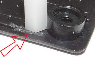
At this point you will note that in the parts there should be a third spacer and countersunk bolt. There is a matching countersunk hole in the lid for these parts This third spacer is used to stop the PCB swivelling, which would occur with just two spacers. This spacer is not bolted to the PCB but is bolted, with a countersunk bolt, to the lid of the case. Trim any leads on the PCB where the third nylon spacer contacts the PCB so the PCB sits level on the three spacers. Before attaching the PCB to the LID, carefully note that there is a lip on the back of the lid (refer to the image at right). Note how the lip may need to be remove so the nylon posts sit vertically. |
|
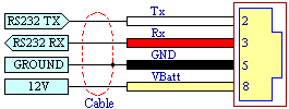
This schematic shows the cable from WBo2 to LD02. Kits are supplied with the shielded 4 core cable pre-crimped to the modular 8 pin RJ45 plug. You should check that the cable has been crimped properly. |

LD02 has a mechanically milled acrylic lens that is glued to the case with craft glue. Many glues (such as super glue & aircraft glues) will damage the acrylic lens. Note: the protective paper covers on the lens are left ON during gluing). 
Begin by obtaining around 180 grit, or finer, sandpaper. Notice that both short edges of the lens have small projections that may need to be removed (they prevent the acrylic moving during milling). Sand just enough from the lens so it fits snugly without being forced (thus distorting the case). Note that the milled hole has a small radius at each corner so chamfer the lens edges with sandpaper to fit. Insert the lens in the case so the outer side of the lens is flush with the label face. This is shown in the image (lower section) at left. The inside edges of the lens should have a lip the glue is applied to. When the fit is correct, insert the lens and apply glue to the edges of the lens from the inside ONLY. This operation is shown at right. Excess glue may spill on the paper, but it can be wiped off while the glue is still tacky. Do not remove the inside protective paper until the glue has dried. After the glue has dried and the top and bottom protective paper covers are removed, the supplied LD02 sticky label can be placed over the lens. Before exposing the label's sticky backing, do a trial run to see exactly where the label is positioned, noting that the button holes will determine the precise location. Discussion of how to use the re-programming interface is described in the |
An important feature of the LD02 is its ability to be re-programmed (reflashed) with updated firmware, and for the display to be set up for different applications. This is achieved by connecting the LD02 to a PC via the adaptor described below.
Note: A very small number of temporary adaptor PCBs were shipped in December '04 & early January '05. If you have one, then you can either have it replaced for free or build and use it - more information here.
|
|
)
)
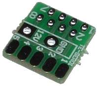
Construction is very simple. The image above right shows the bare PCB. It is labelled as TE-SER01. The three connectors are inserted from the silkscreen side. The overlay for the white Molex® connector is confusing, the top or longest lead from the connector goes to the hole labelled 12V. The female DB9 is soldered directly to the PCB noting that when oriented correctly the 4 pads on the bottom and the 5 pads on the top mate up with the DB9's solder tails. The completed adaptor is shown at left. View it as bigger pop-up. At right the adaptor is shown connected to a PC's RS232 cable (at left), the LD02 (at right), and the power cable from the bottom. View it as an enlarged pop-up. |
The first task is to check your work and carefully examine the PCB for solder shorts, resistor and capacitor leads that are too long and could short, and make sure the diodes D4 and D5 are oriented correctly.
If you have inserted ICs in sockets, carefully remove them (leaving U2 which should be soldered). Make sure the 3 terminal regulator is soldered to the heatsink. Connect LD02 to the programming interface adaptor described above, and apply power. Be ready to measure the voltage at pins 1 and 20 (at the bolt end) of U2 - this should be 5.0 Volts on pin 20.
| 2 | 100 μF Electro | C1, C4 |
| 13 | 100 nF Ceramic/Mono | C2, C3, C5, C6, C7, C8, C10, C12, C13, C14, C15, C18, C19 |
| 2 | 15 pF ceramic | C16, C17 |
| 1 | 10 ohms 1W | R7 |
| 1 | 680 Ohm | R8 |
| 1 | 22 k | R11 |
| 1 | 470 k | R1 |
| 1 | BQ-N516RD = red or FYQ-R1025ZS-11 | D1 | (BQ-N512RD for Green version) = 4 x 7 segment common cathode display or FYQ-5641AUG-11. |
| 2 | BA-10S1UD = red or FYA-R102510ZS-11 | D2, D3 | (BA-10G1UD for Green version) = 10 x bargraph linear display or FYA-R102510ZUG-11. |
| 2 | 1N4007 | D4, D5 | axial GP diode |
| 1 | ATMEGA8 | U1 | DIP-28 |
| 1 | TB62710 | U2 | DIP-20 (nb: no DIP socket used) |
| 1 | TPIC6C595 | U3 | DIP-16 |
| 1 | ST202 | U4 | DIP-16 |
| 1 | 7805 | U5 | D2 PAK packaging |
| 1 | DIP-28 socket | for U1 | |
| 2 | DIP-16 socket | for U3, U4 |
| 1 | PCB | LD02 Main Printed Circuit Board |
| 1 | LDR | LDR Legs need heatshrink |
| 2 | BUTTON | PB1, PB2 3.5 x 6 mm mini press button |
| 8 | 0.1" Machined pins (strip) | 0.1 female pin socket mounts PB1 & PB2 to PCB |
| 1 | 16 MHz | X1 HC49 low profile Crystal |
| 1 | Jumper SHUNT | J1-SHUNT >for two pin Flash/Rescue header |
| 8 | (2+6) 0.1" header (strip) | J1 + Y3 header = 2 for J1, 6 for Y3 |
| 1 | LID | Lid with drilled and countersunk holes |
| 1 | CASE | Machined CASE with cutout for Acrylic lens |
| 1 | Acrylic lens | Red machined acrylic to fit case (Green option) |
| 4 | screws/covers | LID to CASE mounting hardware |
| 3 | 15 mm nylon spacer | PCB to LID mounting supports |
| 3 | M3 countersunk bolts | bolts the spacers to the LID |
| 2 | M3 6 mm bolts | bolts the PCB to the spacers |
| 2 | M3 star washers | securing for PCB to space bolts |
| 1 | Cable | 4 Core main cable with RJ45 |
| 1 | Cable tie | secures the cable to the LID |
| 25 mm | 1.5 mm Heatshrink | for insulating LDR's legs |
| 25 mm | 6 mm Heatshrink | for insulating cable end |
| 1 | wire link | in place of L1 |
| 1 | Reprogrammer PCB | ||
| 1 | Molex 2 pin PCB right angle nylon | power supply connector to battery | |
| 1 | DB9 solder bucket connector | RS232 connector to PC | |
| 1 | RJ45 PCB mount connector | RS232 connector to WBo2 |
We continually update and amend these pages. Please see the contact link below if you find something that needs updating, is in error, or could be explained better.
)
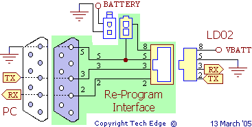
 The re-programming interface adaptor is shown in schematic format at left.
All components on the PCB are shown within the green area.
Connections to the adaptor are shown around the PCB.
The white Molex® two pin socket (top of schematic) connects to the WBo2 power cable (which we assume you are using during re-programming).
The DB9 is for connection to a PC's RS232 cable.
The LD02 itself connects to the 8 pin RJ45 connector (only the RJ45's active 4 pins are shown in the schematic).
The re-programming interface adaptor is shown in schematic format at left.
All components on the PCB are shown within the green area.
Connections to the adaptor are shown around the PCB.
The white Molex® two pin socket (top of schematic) connects to the WBo2 power cable (which we assume you are using during re-programming).
The DB9 is for connection to a PC's RS232 cable.
The LD02 itself connects to the 8 pin RJ45 connector (only the RJ45's active 4 pins are shown in the schematic).
)
)
)
)
)